Introduction
Many devices and protocols use 3.3V logic including I2C and SPI. This logic level converter converts 5V from microcontroller boards like the Arduino UNO to 3.3V and back for use with these systems and devices. Each board has 4 separate channels for converting voltage levels back and forth. It can even be used with 2.8V and 1.8V devices.
In this tutorial we will go over the basics of how the converter works, how to use the converter, and some hookup examples.

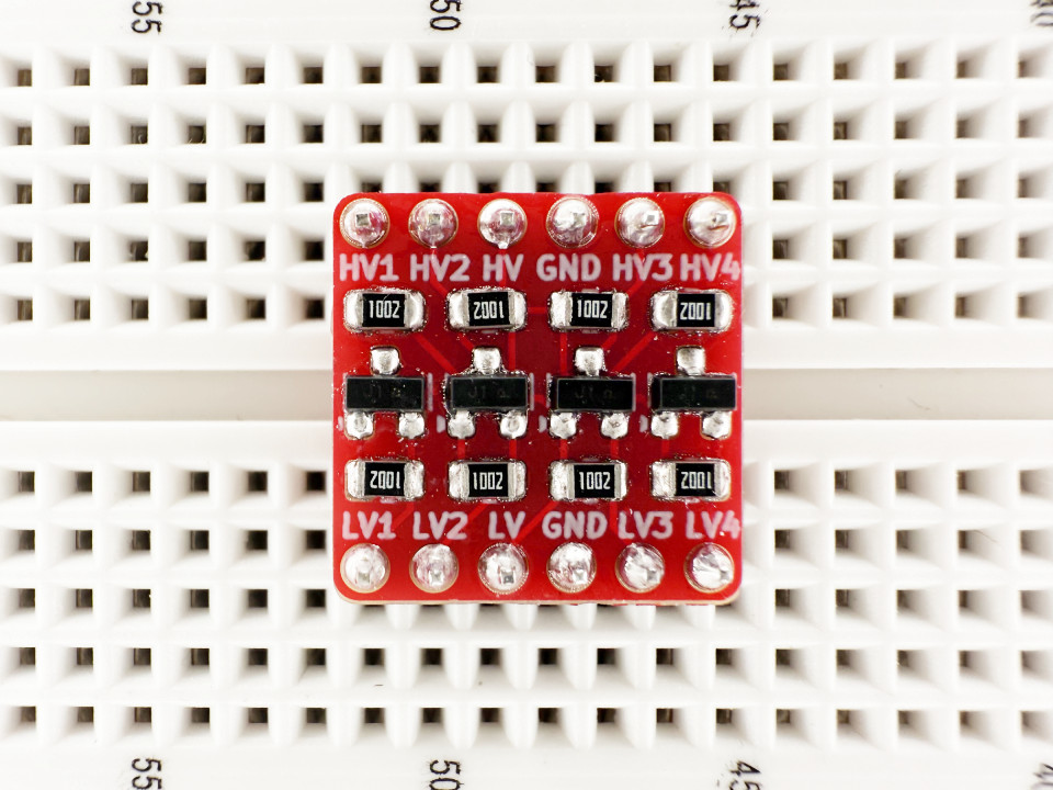
Layout
The board has two rows of pins on it. First, the high voltage pins. They are located on the high side of the board, HV1, HV2, HV, HV3, and HV4. Secondly, the low voltage pins. They are located on the low side of the board, LV1, LV2, LV, LV3, and LV4. There are also GND pins on both of those sides.

There are 4 channels for converting high signals to low signals or vice versa. These channels are marked above, and are labeled with their respective HV and LV numbers (ex. HV1 and LV1). The inputs on the high side and low side are HV, LV, and both GND’s.
Basics of how it works
When HV and LV are powered (LV being a lower voltage than HV), the identical LV voltage on LV1, LV2, LV3, or LV4 will be converted to the higher voltage that HV is powered by. When the identical HV voltage is on HV1, HV2, HV3, or HV4, it will be converted down to the same voltage on the LV pin. Basically, the voltage will be converted back and forth to whatever voltages you connected HV and LV to. The GND pins on the board are simply just connected together and are for ease of use, they are not needed.

Above is the level shifting circuit duplicated 4 times for each of the 4 chanels. It uses 4 BSS138 N-channel MOSFETs to convert the voltage on each channel higher or lower. But for signals at 0V, they will not change in either direction, and will stay at 0V. This circuit is not capable of converting real analog signals, and can only be used with digital signals, like the ones that can come from an Arduino board.
Remember the voltage on the high voltage side should always be higher than on the low voltage side. For example, you can connect 5V to the high side and 3.3V to the low side. Also, It is important to remember that you need to supply both the high voltage and the low voltage, as this board is not a regulator.
How to Use
Start by connecting your high voltage power source (like 5V from an Arduino board) to the HV pin. Don’t connect it to one of the HV channels. Then connect your low voltage power source (like 3.3V from the same Arduino board) to the LV pin. It is important to remember that both these pins need to be powered and won’t convert voltage levels to each other.
After this you can connect your low voltage device data pins to one or more of the channel pins on the LV side. For example, connecting 3.3V SDA to LV1 and 3.3V SCL to LV2. You can then connect the data pins of your high voltage device to the respective channel pins on the high side. For example, 5V SDA to HV1 and 5V SCL to HV2. Note that both GND pins on the board do not need to be used, and instead both of the HV and LV device’s GND’s can be directly connected together.
Below is an example of 5V logic from a Nano clone board connected to the logic level converter, which is then connected to a QWIIC adapter. The 5V SDA/SCL from the Nano board is converted down to 3.3V SDA/SDL to use with the QWIIC ecosystem.

A schematic is shown below for easier wiring reference.

The wiring from the Nano board to the logic level converter goes: 5V to HV, 3.3V to LV, A4 (SDA) to HV2, and finally A5 (SCL) to HV1. The wiring of the QWIIC adapter goes: SDA to LV2 of the logic level converter (LLC), SCL to LV1 of the LLC, 3.3V to 3.3V on the Nano, and GND to GND on the Nano. The LV pin of the LLC is also connected to 3.3V.
Wiring this way turns the 5V SDA and SCL lines from the Nano board to 3.3V so you can use 3.3V I2C devices with 5V ones.


Leave a Reply